Samsung to Use TSMC’s 3-Nanometre Process for Nvidia Memory
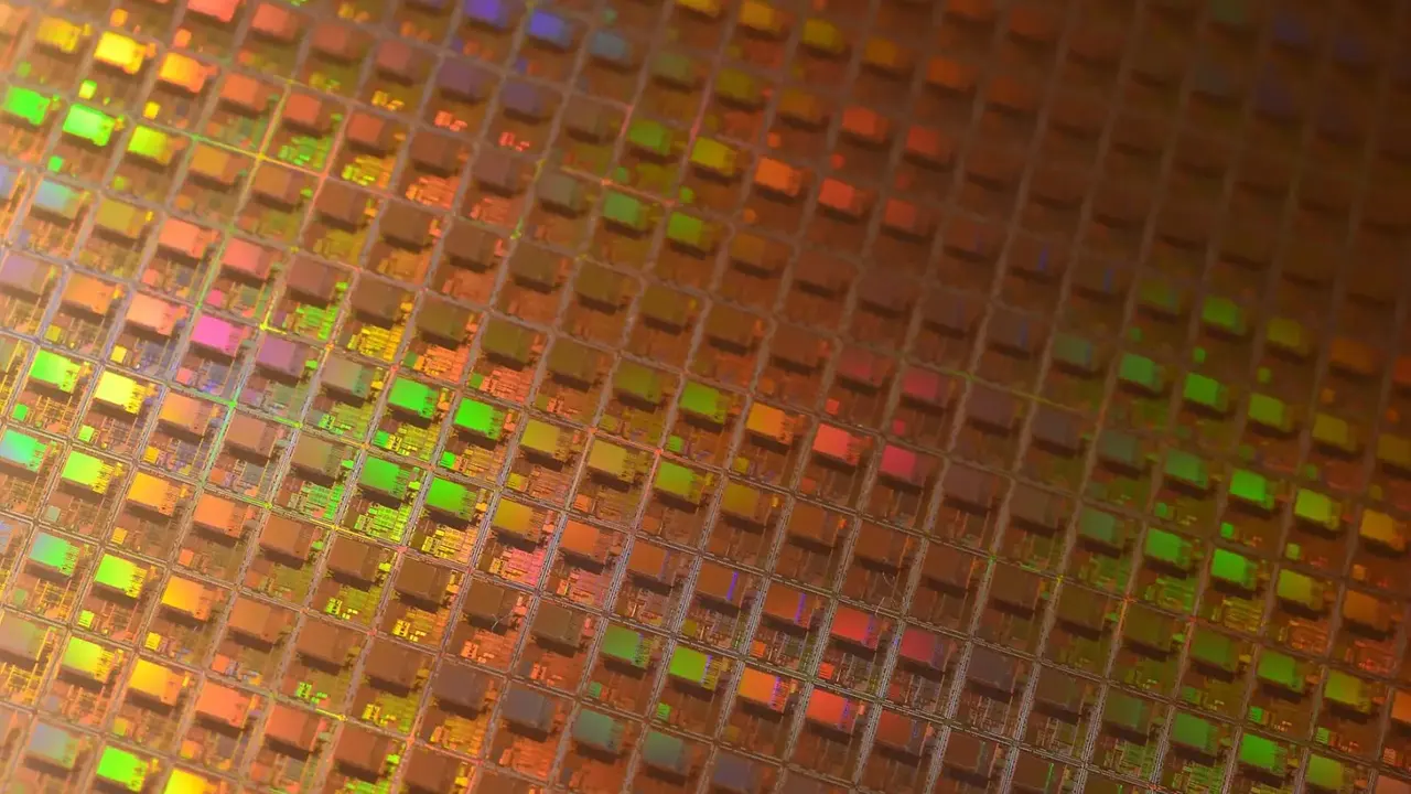
Samsung accepted Nvidia’s requirements for custom memory chips while keeping its own production approach for standard HBM and other customers.
Key takeaways
- Samsung plans to use TSMC’s 3-nanometre process for Nvidia’s custom HBM base dies.
- Samsung will retain its in-house production model for standard HBM and custom products for other customers.
Samsung Electronics plans to use TSMC’s 3-nanometre process to make base dies for Nvidia’s next-generation custom high-bandwidth memory chips, the Seoul Economic Daily reported Sunday.
Nvidia asked Samsung, SK Hynix and Micron Technology to use the process for the base dies and sixth-generation DRAM for the chips’ core dies, the newspaper reported, citing industry sources. Samsung accepted the requirements after an internal review, according to the report.
Samsung plans to keep its in-house production model for standard HBM and custom products for other customers. It is also assessing whether its own foundry could make the base dies if demand exceeds TSMC’s capacity, the newspaper reported.
This article was produced with the help of AI technology. Based on reporting by the outlets listed above.